Midterm February 28, 2015 Name ____________________________________ Student ID __________________
1.3 Which waveform is the result of the simulation below?
module design (input a, input b, output o);
assign o = a & b;
endmodule
module tb;
logic a, b, o;
design design_inst (a, b, o);
initial
begin
$dumpvars;
$monitor ("%t a %b b %b o %b", $time, a, b, o);
#10;
a = 0; b = 0; #10;
a = 1; b = 0; #10;
a = 0; b = 1; #10;
a = 1; b = 1; #10;
end
endmodule
a)
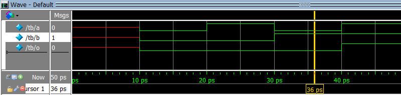 b)
b)
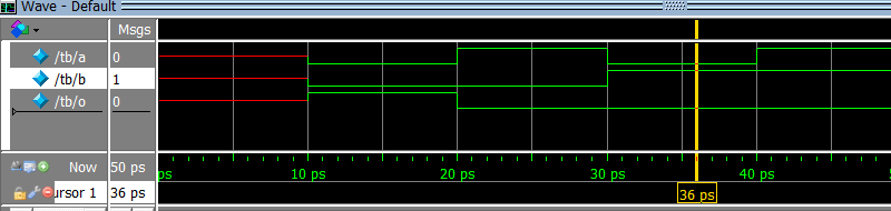 c)
c)
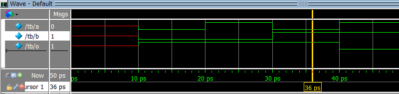 d)
d)
 e)
e)
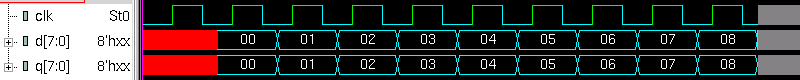
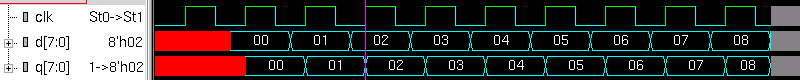
 2.3 Which waveform is the simulation result of Verilog code below?
module dut
(
input clk,
input [7:0] d,
output logic [7:0] q
);
always @*
q = d;
endmodule
module testbench;
logic clk;
logic [7:0] d, q;
dut dut (clk, d, q);
initial
begin
clk = 0;
forever
#10 clk = ! clk;
end
initial
begin
$dumpvars ();
for (int i = 0; i < 10; i++)
begin
@(posedge clk);
#15;
d = i;
end
$finish;
end
endmodule
a)
2.3 Which waveform is the simulation result of Verilog code below?
module dut
(
input clk,
input [7:0] d,
output logic [7:0] q
);
always @*
q = d;
endmodule
module testbench;
logic clk;
logic [7:0] d, q;
dut dut (clk, d, q);
initial
begin
clk = 0;
forever
#10 clk = ! clk;
end
initial
begin
$dumpvars ();
for (int i = 0; i < 10; i++)
begin
@(posedge clk);
#15;
d = i;
end
$finish;
end
endmodule
a)
 b)
b)
 c)
c)
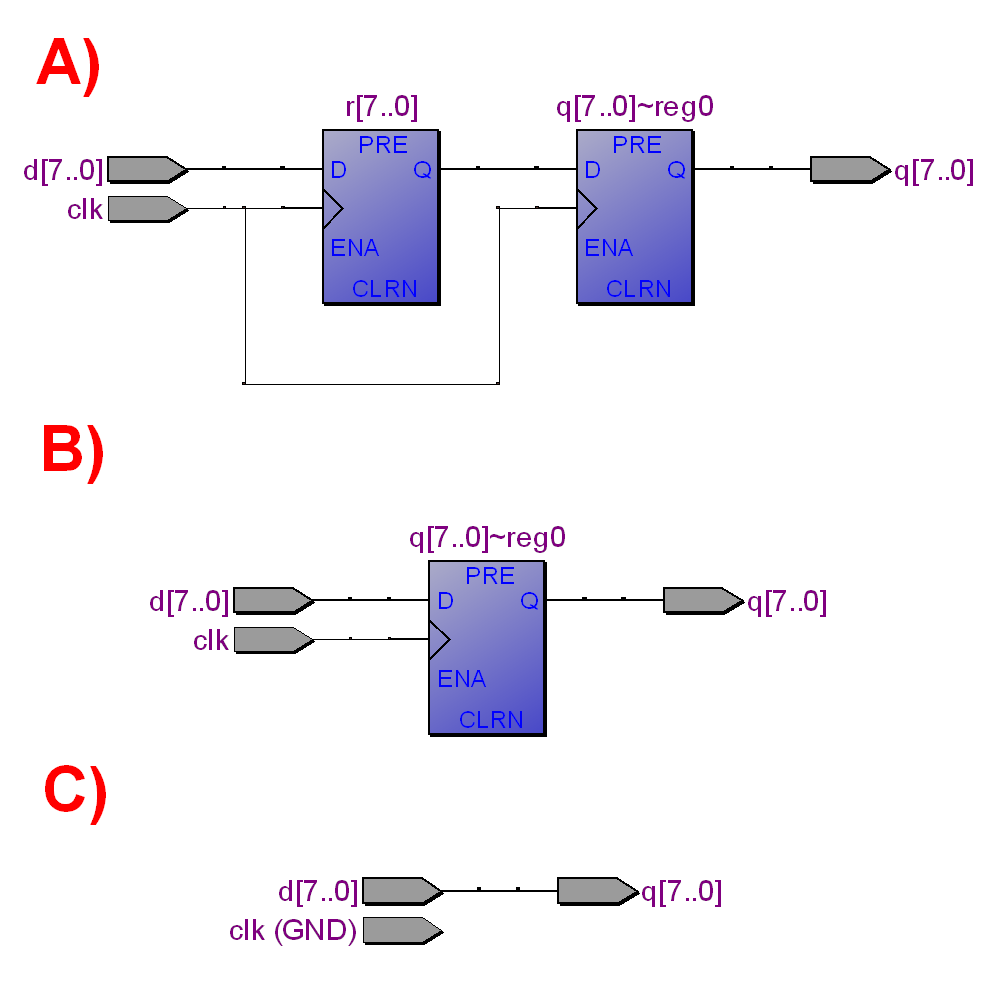
 3.3 What schematics correspond to Verilog code below?
module dut
(
input clk,
input [7:0] d,
output logic [7:0] q
);
logic [7:0] r;
always @(posedge clk)
begin
r <= d;
q <= r;
end
endmodule
3.3 What schematics correspond to Verilog code below?
module dut
(
input clk,
input [7:0] d,
output logic [7:0] q
);
logic [7:0] r;
always @(posedge clk)
begin
r <= d;
q <= r;
end
endmodule
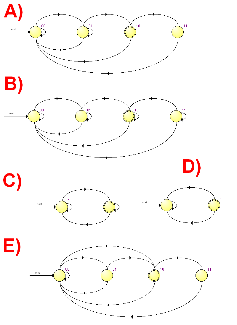
 4.3 What Finite State Machine (FSM) state diagram correspond to Verilog code below?
module dut
(
input clk,
input resetn,
input a,
output b
);
logic [1:0] state;
always @(posedge clk)
if (! resetn)
state <= 0;
else
case (state)
0: if ( a) state <= 1;
1: if (! a) state <= 2;
2: if ( a) state <= 3;
3: if (! a) state <= 0;
endcase
assign b = (state == 2);
endmodule
4.3 What Finite State Machine (FSM) state diagram correspond to Verilog code below?
module dut
(
input clk,
input resetn,
input a,
output b
);
logic [1:0] state;
always @(posedge clk)
if (! resetn)
state <= 0;
else
case (state)
0: if ( a) state <= 1;
1: if (! a) state <= 2;
2: if ( a) state <= 3;
3: if (! a) state <= 0;
endcase
assign b = (state == 2);
endmodule
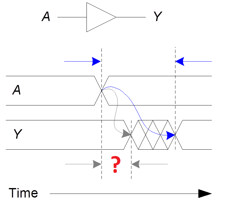
 5.3 What kind of delay is illustrated on the picture below (marked by "?")?
a) Propagation delay: tpd = max delay from input to output
b) Contamination delay: tcd = min delay from input to output
c) Skew: difference between two clock edges. The clock doesn’t arrive at all registers at same time
5.3 What kind of delay is illustrated on the picture below (marked by "?")?
a) Propagation delay: tpd = max delay from input to output
b) Contamination delay: tcd = min delay from input to output
c) Skew: difference between two clock edges. The clock doesn’t arrive at all registers at same time
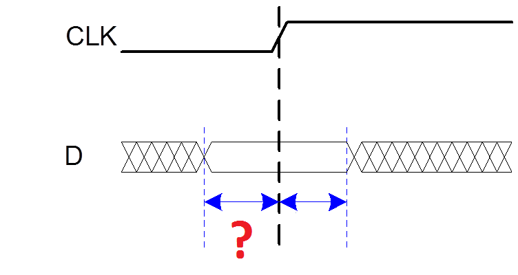
 6.3 What kind of timing constraint is illustrated on the picture below (marked by "?")?
a) Setup time: tsetup = time before clock edge data must be stable (i.e. not changing)
b) Hold time: thold = time after clock edge data must be stable
c) Aperture time: ta = time around clock edge data must be stable (ta = tsetup + thold)
d) Tc = minimum and maximum delays between registers
6.3 What kind of timing constraint is illustrated on the picture below (marked by "?")?
a) Setup time: tsetup = time before clock edge data must be stable (i.e. not changing)
b) Hold time: thold = time after clock edge data must be stable
c) Aperture time: ta = time around clock edge data must be stable (ta = tsetup + thold)
d) Tc = minimum and maximum delays between registers
 7.3 Which rule for signal assignment is violated in the following code?
a) Synchronous sequential logic: use always @(posedge clk) or always_ff @(posedge clk)
and nonblocking assignments (<=)
always_ff @ (posedge clk)
q <= d; // nonblocking
b) Simple combinational logic: use continuous assignments (assign…)
assign y = a & b;
c) More complicated combinational logic: use always @* or always_comb and blocking assignments (=)
d) Assign a signal in only one always statement or continuous assignment statement
e) This code does not violate any rules for signal assignment
module isqrt
(
input clock,
input reset_n,
input run,
input [31:0] x,
output reg ready,
output reg [15:0] y
);
reg [31:0] m, r_m;
reg [31:0] tx, r_tx;
reg [31:0] ty, r_ty;
reg [31:0] b, r_b;
reg new_ready;
always @*
begin
if (run)
begin
m = 31'h4000_0000;
tx = x;
ty = 0;
end
else
begin
m = r_m;
tx = r_tx;
ty = r_ty;
end
b = ty | m;
ty = ty >> 1;
if (tx >= b)
begin
tx = tx - b;
ty = ty | m;
end
new_ready = m [0];
m = m >> 2;
end
always @(posedge clock or negedge reset_n)
begin
if (! reset_n)
begin
ready <= 0;
y <= 0;
end
else if (new_ready)
begin
ready <= 1;
y <= ty [15:0];
end
else
begin
ready <= 0;
r_m <= m;
r_tx <= tx;
r_ty <= ty;
r_b <= b;
end
end
endmodule
8.3 Suppose you are using the following module
to generate low-frequency clock using 80 MHz clock.
What will be the resulting frequencies
of clock_for_debouncing and clock_for_display?
a) 47.6 Hz and 763 Hz
b) 95.3 Hz and 1.53 KHz
c) 76.2 Hz and 1.22 KHz
d) 7.63 Hz and 122 Hz
e) 23.8 Hz and 381 Hz
module clock_divider
(
input clock,
input reset,
output clock_for_debouncing,
output clock_for_display
);
reg [19:0] counter;
always @(posedge clock)
begin
if (reset)
counter <= 0;
else
counter <= counter + 1;
end
assign clock_for_debouncing = counter [19];
assign clock_for_display = counter [15];
endmodule
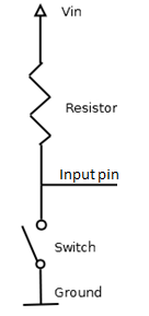
9.3 What is the function of the resistor in this particular circuit?
a) To protect LED from excessive current
b) Pullup - to provide the default value 1 for the input
c) Pulldown - to provide the default value 0 for the input
d) All the above
e) This resistor does not have any function in this circuit
7.3 Which rule for signal assignment is violated in the following code?
a) Synchronous sequential logic: use always @(posedge clk) or always_ff @(posedge clk)
and nonblocking assignments (<=)
always_ff @ (posedge clk)
q <= d; // nonblocking
b) Simple combinational logic: use continuous assignments (assign…)
assign y = a & b;
c) More complicated combinational logic: use always @* or always_comb and blocking assignments (=)
d) Assign a signal in only one always statement or continuous assignment statement
e) This code does not violate any rules for signal assignment
module isqrt
(
input clock,
input reset_n,
input run,
input [31:0] x,
output reg ready,
output reg [15:0] y
);
reg [31:0] m, r_m;
reg [31:0] tx, r_tx;
reg [31:0] ty, r_ty;
reg [31:0] b, r_b;
reg new_ready;
always @*
begin
if (run)
begin
m = 31'h4000_0000;
tx = x;
ty = 0;
end
else
begin
m = r_m;
tx = r_tx;
ty = r_ty;
end
b = ty | m;
ty = ty >> 1;
if (tx >= b)
begin
tx = tx - b;
ty = ty | m;
end
new_ready = m [0];
m = m >> 2;
end
always @(posedge clock or negedge reset_n)
begin
if (! reset_n)
begin
ready <= 0;
y <= 0;
end
else if (new_ready)
begin
ready <= 1;
y <= ty [15:0];
end
else
begin
ready <= 0;
r_m <= m;
r_tx <= tx;
r_ty <= ty;
r_b <= b;
end
end
endmodule
8.3 Suppose you are using the following module
to generate low-frequency clock using 80 MHz clock.
What will be the resulting frequencies
of clock_for_debouncing and clock_for_display?
a) 47.6 Hz and 763 Hz
b) 95.3 Hz and 1.53 KHz
c) 76.2 Hz and 1.22 KHz
d) 7.63 Hz and 122 Hz
e) 23.8 Hz and 381 Hz
module clock_divider
(
input clock,
input reset,
output clock_for_debouncing,
output clock_for_display
);
reg [19:0] counter;
always @(posedge clock)
begin
if (reset)
counter <= 0;
else
counter <= counter + 1;
end
assign clock_for_debouncing = counter [19];
assign clock_for_display = counter [15];
endmodule
9.3 What is the function of the resistor in this particular circuit?
a) To protect LED from excessive current
b) Pullup - to provide the default value 1 for the input
c) Pulldown - to provide the default value 0 for the input
d) All the above
e) This resistor does not have any function in this circuit
 Test written by Yuri Panchul
Sources of pictures:
Slides from Steve Harris and Sarah Harris that accompany textbook
Digital Design and Computer Architecture, Second Edition by David Harris and Sarah Harris, 2012
http://tinkerlog.com/2009/04/05/driving-an-led-with-or-without-a-resistor/
http://learn.sparkfun.com/tutorials/pull-up-resistors
http://ieeetamu.org/mcc/wsref/
Test written by Yuri Panchul
Sources of pictures:
Slides from Steve Harris and Sarah Harris that accompany textbook
Digital Design and Computer Architecture, Second Edition by David Harris and Sarah Harris, 2012
http://tinkerlog.com/2009/04/05/driving-an-led-with-or-without-a-resistor/
http://learn.sparkfun.com/tutorials/pull-up-resistors
http://ieeetamu.org/mcc/wsref/